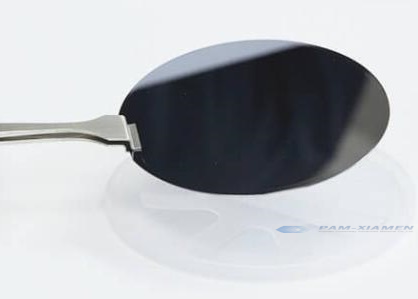
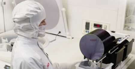
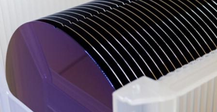
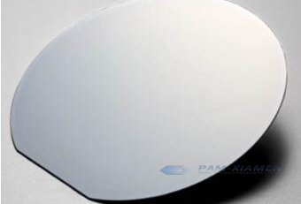
Detector Epitaxy Wafer
Group III-V compounds, especially gallium arsenide (GaAs), indium phosphide (InP), etc., are direct band gap materials. The top of the valence band and the bottom of the conduction band are located at the same position in the wave vector k-space. Recombination of electrons and holes do not need to exchange momentum, so there will be high internal quantum efficiency. Both GaAs and InP can be used to fabricate detectors. The InP-based epitaxy wafer for PIN detectors and avalanche detectors (APD) are mainly prepared by the MOCVD. Generally, the epi growth wafer does not contain high-concentration p-type doping. For detector epitaxial wafer manufacturers, Zn diffusion is a common means to make the p-type InP or InGaAs ohmic contact layer required for device fabrication.
1. Specification of InGaAs Detector Epitaxy Wafer
InP Mobility >4000cm2/ (V·s) @ RT, UID <2E15cm-3;
InGaAs Mobility >10000 cm2/ (V·s) @ RT, UID< 1E 15 cm-3;
Non-uniformity of thickness <±1%;
Non-uniformity of composition (In 0.53Ga 0.47As) <± 1.5%;
The density of surface defect (Size >2um) <10/cm2;
Non-uniformity of doping < ± 1% E18
2. Comparison for Detector Epitaxy Wafer between APD and PIN
InGaAs wafer epitaxy is used to fabricate many detectors, such as InGaAs PIN detectors, InGaAs APD detectors, InGaAs Schottky detectors and quantum well detectors, etc.
Generally speaking, APD on InP epi wafer is suitable for long-distance transmission and high-speed communication systems that require high receiving sensitivity; while PIN based on InGaAs/InP epitaxial wafer is suitable for medium and short distance and medium and low speed systems, especially PIN/FET components are widely used.
Therefore, high-sensitivity detection materials, such as III-V epitaxial wafers of InGaAs/InP, are more suitable use as in the 1310 ~ 1550nm band of infrared communication. The APD produced on InGaAs/InP material system has higher quantum efficiency and lower dark current noise.
3. Advantages of Detector based on InGaAs Epitaxial Wafer
InGaAs has higher electron mobility and lower lattice mismatch, and can work at room temperature and near room temperature. The InGaAs wafer epitaxy process is more mature, and its response band can also be extended to visible light. Therefore, the detector made of InGaAs epitaxy semiconductor not only has the excellent characteristics of good IV characteristics, low dark current, low blind element rate, and high sensitivity, but also has the characteristics of higher operating temperature, low component power consumption, small weight, and long life.
4. Challenges for the Expansion of Near-Infrared InGaAs Detectors
Traditional PIN-type InGaAs epitaxial film wafer include InP substrate, InGaAs absorber layer and InP cap layer.
The band gap of InP is 1.35eV, and the corresponding cut-off wavelength is 920nm. The band gap of In0.53Ga0.47As is 0.75eV, and the corresponding cut-off wavelength is 1700nm. Due to the absorption of the InP cap layer or the substrate of epitaxy wafer, the detection range of the traditional InGaAs detector is 0.9-1.7 m. For the InGaAs area array detector, the back-illuminated working mode is adopted. Therefore, in order to extend the response wavelength of the detector to visible light, the InP substrate needs to be thinned or removed during the device fabrication.
Therefore, it is firstly necessary to find a suitable method to remove the InP substrate, to ensure that the chip surface is uniform after thinning, and the damage and stress caused to the device are small.
Secondly, determine the thickness of InP that needs to be thinned in the epi wafer manufacturing process, and study the transmittance of the InP layer on the epitaxy wafer in the short-wave infrared and visible light bands.
Thirdly, InP is lattice-matched with In0.53Ga0.47As. In order to ensure the performance of the thinned device, a certain thickness of InP layer needs to be reserved as the surface passivation layer. The process characteristics of InGaAs also determine that the InP layer is required to provide a common cathode contact. This puts forward further requirements for epitaxial wafer suppliers on the thinning method.
Fourth, in the process of thinning the bottom of the InP substrate, the thickness of the epitaxial wafer growing chip is only a few micrometers left, which is very easy to be broken and can no longer be patterned, and the process flow of the detector needs to be adjusted.
Fifth, after thinning the device substrate, considering the increase in surface leakage and increasing the dark current of the device, surface passivation needs to be considered. In order to improve the quantum efficiency of the device, an anti-reflection coating is required and the influence of growing the antireflection coating on the quantum efficiency in the visible and near-infrared bands needs to be considered.
Finally, in the process of expanding to the visible, the structure of detector epitaxy wafer was changed to improve the quantum efficiency of the visible band while ensuring the good performance of the detector in the short-wave infrared band.
For more information, please contact us email at sales@ganwafer.com and tech@ganwafer.com.

