1240nm InP Laser Diode Structures
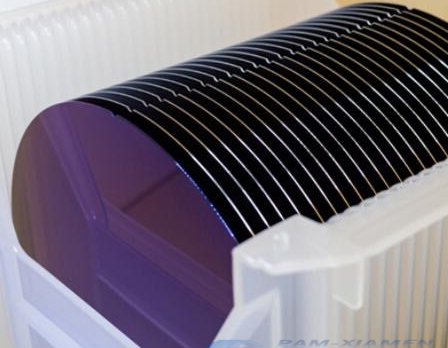
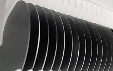
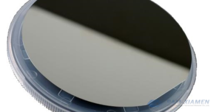
InP (Indium Phosphide) material system includes ternary and quaternary III-V semiconductor materials, such as InGaAs, InGaAsP, InAlGaAs and InAlAsP, which are lattice matched to InP substrate. Among them, quaternary alloy of InAlGaAs lattice matched to InP is an important material for optoelectronic devices. Ganwafer can provide InP laser wafer of Grinsch (GRIN) structure with InAlGaAs epilayers as follows:
1. InGaAlAs / InP Laser Epi Structures
No.1 Epi Laser on InP Substrate
GANW200729-1240nmLD
| 1 | InP Substrate
(Material no.:M01*) |
S-Dopded
2~8 x 10¹⁸ |
cm-3 |
| 2 | N-InP Buffer Layer
(Concentration) |
– | um
(cm-3) |
| 3 | N-InAlAs Layer
(Concentration) |
– | um
(cm-3) |
| 4 | U-GRIN AlQ (AlT to 0.96) | 0.1 um | um |
| 5 | 5 x QW / 6 x Barrier
(λPL=1248.5 nm) |
– | nm
(nm) |
| 6 | U-GRIN AlQ (0.96 to AlT) | – | um |
| 7 | U-InAlAs Layer | – | um |
| 8 | P-InP Layer
(Concentration) |
– | um
(cm-3) |
| 9 | P-1.1um InGaAsP
(Concentration) |
– | um
(cm-3) |
| 10 | P-InP Layer
(Concentration) |
– | um
(cm-3) |
| 11 | P-InGaAsP Layer
(Concentration) |
– | um
(cm-3) |
| 12 | P-InGaAs Layer
(Concentration) |
0.2 um
(>1 x 10¹⁹) |
um
(cm-3) |
| 13 | Lattice mismatch | <±500 | ppm |
No.2 Laser Structure with InAlGaAs QW
GANW200730-1240nmLD
| Layer No. | Material | d (nm) | Depth (nm) | Doping (cm) |
| 1 | n – InP 3″ Substrate (S-doped) | n=2-8e18 | ||
| 2 | n – lnP | – | – | – |
| 3 | n – InAlAs | – | – | – |
| 4 | u-GRIN AIQ (0.96 to AIT) | – | – | N/A |
| 5 | 6 x u-InAlGaAs QW (+1% CS)/
5 x u-InAlGaAs Barrier (-0.5% TS) |
– | – | N/A |
| 6 | u-GRIN AIQ (AIT to 0.96) | – | – | N/A |
| 7 | u- InAlAs | – | 962.5 | N/A |
| 8 | p-InP | – | – | – |
| 9 | p+-1.3 um InGaAsP (LM) | – | – | – |
| 10 | p+-1.5 um InGaAsP (LM) | – | – | – |
| 11 | p++- InGaAs- Cap | 100 | – | p>1e19 |
Remark: GRIN AlQ (AlT to 0.96): Layers of No.4 and No.6 are graded waveguide layers, and the composition change from InAlAs to InAlGaAs with wavelength of 0.96um.
It has been reported that laser structure based on GRIN-SCH has various advantages over STEP-SCH-based nanostructures, such as higher injection efficiency, higher trapping efficiency, significantly shorter doping time and enhanced carrier confinement.
2. InAlGaAs Material for InP Laser Diode
In terms of InAlGaAs / InAlAs heterostructure on InP, the bandgap energy can be revised between that of In0.53Ga0.47As and In0.52Al0.48As. Moreover, InAlGaAs is easier growing by MBE. There is only one V group element. Therefore, the alloy composition can be easily changed by adjust the Group III beam equivalent pressure ratio, better controlling the ratio of As/P during the growth of InGaAsP.
The refractive index ratio between waveguide and cladding of InAlGaAs / InP heterostructure is higher than that of InGaAsP / InP with identical bandgap, making InAlGaAs more attractive than InGaAsP in various applications. In addition, the bandgap of InAlGaAs can be varied easily, but the lattice still matches to InP wafer during the epitaxial growth. The AlGaInAs / InP material system was introduced into the active region because the higher optical can be obtained. Therefore, InAlGaAs material plays more and more important role in manufacturing long wavelength semiconductor waveguide devices (e.g. InP laser fabrication).
For more information, please contact us email at sales@ganwafer.com and tech@ganwafer.com.

