InSb Semiconductor Wafer
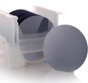
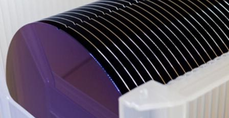
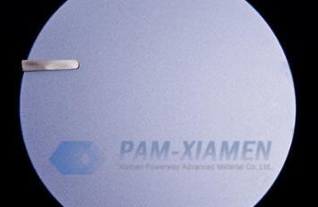
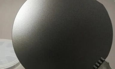
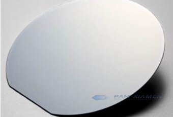
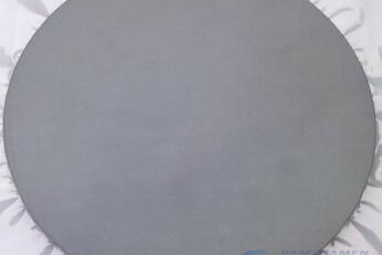
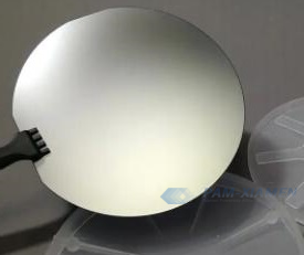
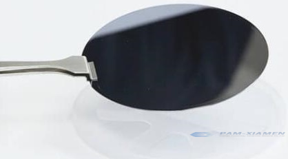
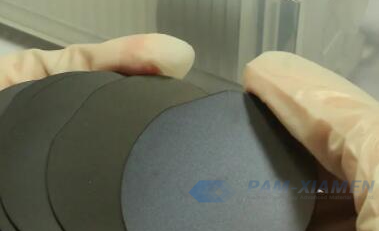
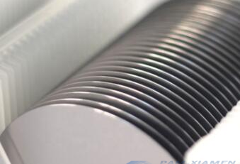
Indium antimonide (InSb) is III-V compound semiconductor material with extremely narrow band gap, extremely small electron effective mass and extremely high electron mobility. Due to its excellent and stable physical and chemical properties, InSb semiconductor material has gained important applications in industrial technology fields such as Hall devices and magnetoresistive sensor. It is particularly noteworthy that InSb is intrinsically absorbed in the 3-5um band, so InSb detectors have extremely high quantum efficiency and responsivity, making InSb crystal the preferred material for mid-wave infrared detectors. Ganwafer can offer InSb wafer for HC chip, and details as follows:
1. Specification of InSb Compound Wafer
|
InSb Wafer for HC Chip GANW160517-INSB |
|
| Material | InSb |
| Dopant | Te N-type |
| Orientation | (111)B±0.1° |
| Diameter/dimensions(mm) | 50.5±0.5 |
| Flat Option(EJ/SEMI) | 2 Flats at 120° |
| Major Flat Length(mm) | 16±2 on (01-1) |
| Minor Flat Length(mm) | 8±1 on (1-10) |
| Surface Finish | SSP |
| Thickness(microns) | 500±25 |
| BOW(microns) | <10 |
| Warp(microns) | <10 |
| TTV(microns) | <5 |
| Carrier concentration (㎤) | E14~E15 |
| Average EPD(㎠) | <=50 |
Mark:The electrical signal is related to the level of carrier concentration of single crystal InSb substrate. But the substrate concentration of E14 cm-3 is too low to determine some signals. To get higher concentration (e.g. E15~E16 cm-3) to determine electrical signals, the InSb compound substrate should be doped with Te, and the purity should be over 6N.
2. Chemical Corrosion of InSb Semiconductor Substrate
Chemical etching is one of the commonly used surface treatment methods in the device manufacturing process. InSb material belongs to III-V semiconductors. Due to the difference in chemical properties between subgroup elements and V group elements in compound semiconductor materials, the chemical corrosion of InSb material is more complicated than that of silicon material.
Due to the difference in bond density, the InSb (111) plane will form (111) A plane and (111) B plane, each of which is completely composed of In atoms or completely composed of Sb atoms. The atomic order of the (111)A plane is first a planar In atom followed by a planar Sb atom. On the opposite (111) B face, the atomic order is reversed, first a planar Sb atom and then a planar In atom. It is because of this structure that the [111] direction is called the polar axis. Studies of InSb substrate have shown that the existence of the polar axis leads to two opposite (111) crystal planes having different behaviors in some physicochemical processes.
For InSb semiconductor, it has been reported that they exhibit different piezoelectric effects during dislocation corrosion, different rates of anodic oxidation, and different thicknesses of oxide layers formed by anodic and chemical oxidation, and different corrosion rates and corrosion rates. The pits are of different shapes.
3. Indium Antimonide Wafer Cutting
At present, InSb wafers are mostly cut by inner circle, which has the advantages of convenient operation and mature technology. In recent years, researchers at home and abroad have conducted in-depth research on the damage and mechanism of the inner circle cut InSb semiconductor wafer. The damage layer is considered to be composed of two-layer lattice imperfections: the outer layer is the fracture layer, including microcracks, fractures and defects, and the stress layer below the fracture layer, and the microcracks of the fractured layer are the main reason for the great reduction of the mechanical strength of the InSb wafers.
However, with the continuous increase of the diameter and length of bulk semiconductor indium antimonide, especially for InSb crystals above 4 inches, the inner circle cutting has obvious shortcomings in terms of processing efficiency and processing loss. Currently, the diameter of the blade line of wire cutting is generally less than 150um; while the thickness of the blade of the inner circle cutting machine is 300um, which is significantly wider than the diameter of the blade line. The cutting line of the multi-wire cutting machine is wound into multiple parallel cutting lines through a complex mechanical mechanism, which can be cut at the same time each time. The processing efficiency is dozens of times that of the inner circular cutting machine. Wire cutting is more suitable for the production and processing of large-size, large-volume InSb substrates.
The degree of surface damage of wire-cut single crystal InSb wafers and inner circle-cut wafers was observed by Scanning Electron Microscopy (SEM), step meter and X-ray Diffraction (XRD), and the thickness of the damaged layer was quantitatively analyzed. The results show that the surface of the wire-cut InSb semiconductor wafer is relatively flat, the roughness is small, and the surface damage is small.
For more information, please contact us email at sales@ganwafer.com and tech@ganwafer.com.

