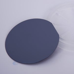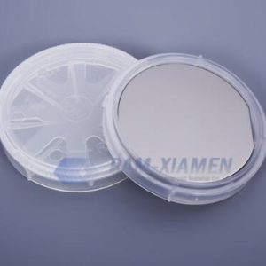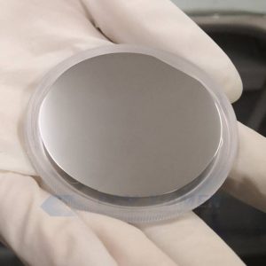
InAs Wafer
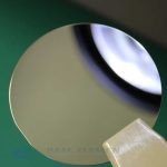
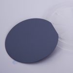
Compound semiconductor indium arsenide (InAs) wafer for sale is composed of indium and arsenic III-V elements grown by LEC (Liquid Encapsulated Czochralski). Ganwafer offers indium arsenide substrate in epi-ready or mechanical grade with n type, p type or semi-insulating in different orientations as terahertz radiation source.
Indium arsenide compound semiconductor is a direct bandgap material, which is similar to gallium arsenide (GaAs). Sometimes, InAs is used with InP. InAs is alloyed with GaAs forming indium gallium arsenide. More specifications of indium arsenide wafer please see as follows:
- Description
- Inquiry
Description
1. Specifications of InAs Wafer
1.1. 4″ Indium Arsenide Wafer Specification
| Item | Specifications | |||
| Dopant | low doped | Stannum | Sulphur | Zinc |
| Conduction Type | N-type | N-type | N-type | P-type |
| Wafer Diameter | 4″ | |||
| Wafer Orientation | (100)±0.5° | |||
| Wafer Thickness | 900±25um | |||
| Primary Flat Length | 16±2mm | |||
| Secondary Flat Length | 8±1mm | |||
| Carrier Concentration | 5×1016cm-3 | (5-20)x1017cm-3 | (1-10)x1017cm-3 | (1-10)x1017cm-3 |
| Mobility | ≥2×104cm2/V.s | 7000-20000cm2/V.s | 6000-20000cm2/V.s | 100-400cm2/V.s |
| EPD | <5×104cm-2 | <5×104cm-2 | <3×104cm-2 | <3×104cm-2 |
| TTV | <15um | |||
| BOW | <15um | |||
| WARP | <20um | |||
| Laser marking | upon request | |||
| Surface finish | P/E, P/P | |||
1.2. 3″ Indium Arsenide Substrate Specification
| Item | Specifications | |||
| Dopant | low doped | Stannum | Sulphur | Zinc |
| Conduction Type | N-type | N-type | N-type | P-type |
| Wafer Diameter | 3″ | |||
| Wafer Orientation | (100)±0.5° | |||
| Wafer Thickness | 600±25um | |||
| Primary Flat Length | 22±2mm | |||
| Secondary Flat Length | 11±1mm | |||
| Carrier Concentration | 5×1016cm-3 | (5-20)x1017cm-3 | (1-10)x1017cm-3 | (1-10)x1017cm-3 |
| Mobility | ≥2×104cm2/V.s | 7000-20000cm2/V.s | 6000-20000cm2/V.s | 100-400cm2/V.s |
| EPD | <5×104cm-2 | <5×104cm-2 | <3×104cm-2 | <3×104cm-2 |
| TTV | <12um | |||
| BOW | <12um | |||
| WARP | <15um | |||
| Laser marking | upon request | |||
| Surface finish | P/E, P/P | |||
| Epi ready | yes | |||
| Package | Single wafer container or cassette | |||
| Epi ready | yes | |||
| Package | Single wafer container or cassette | |||
1.3. 2″ Compound Semiconductor InAs Wafer Specification
| Item | Specifications | |||
| Dopant | low doped | Stannum | Sulphur | Zinc |
| Conduction Type | N-type | N-type | N-type | P-type |
| Wafer Diameter | 2″ | |||
| Wafer Orientation | (100)±0.5° | |||
| Wafer Thickness | 500±25um | |||
| Primary Flat Length | 16±2mm | |||
| Secondary Flat Length | 8±1mm | |||
| Carrier Concentration | 5×1016cm-3 | (5-20)x1017cm-3 | (1-10)x1017cm-3 | (1-10)x1017cm-3 |
| Mobility | ≥2×104cm2/V.s | 7000-20000cm2/V.s | 6000-20000cm2/V.s | 100-400cm2/V.s |
| EPD | <5×104cm-2 | <5×104cm-2 | <3×104cm-2 | <3×104cm-2 |
| TTV | <10um | |||
| BOW | <10um | |||
| WARP | <12um | |||
| Laser marking | upon request | |||
| Surface finish | P/E, P/P | |||
| Epi ready | yes | |||
| Package | Single wafer container or cassette | |||
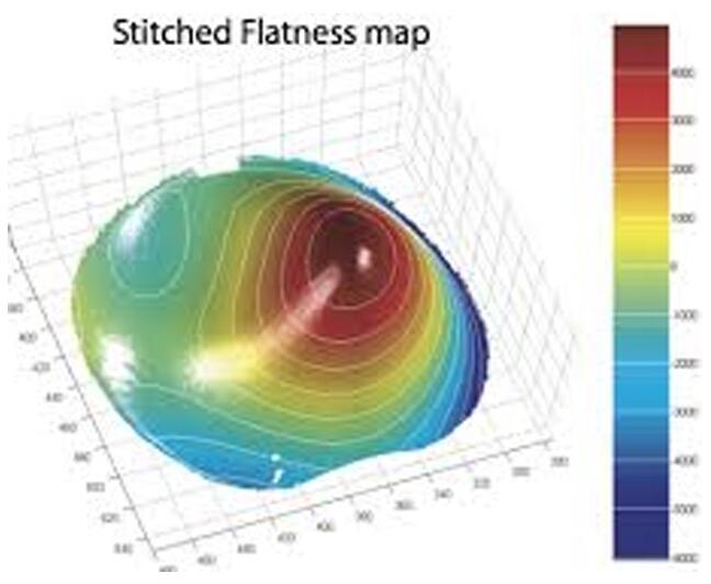
2. Stitched Flatness Map of InAs Wafer:
3. Indium Arsenide Applications
Indium arsenide crystal has high electron mobility and mobility ratio (μe/μh=70), low magneto resistance effect and small temperature coefficient of resistance. Thus, indium arsenide solution is an ideal for manufacturing Hall devices and magneto-resistive devices.
Single crystal InAs substrate can grow InAsSb/InAsPSb, InAsPSb and other heterostructure materials to produce infrared light-emitting devices with a wavelength of 2-12um.
Indium Arsenides single crystal substrates can also be used to epitaxially grow InAsPSb superlattice structure materials to produce mid-infrared quantum cascade lasers. These infrared devices have good application prospects in the fields of gas detection and low-loss optical fiber communication.
4. Influence of Annealing Process on Surface Electron Accumulation Layers of InAs Wafer
Use Raman spectroscopy to investigate the effect of annealing temperature on optical properties of n type (100) indium arsenide wafer surface electron accumulation layers. The result shows the Raman peaks caused by unscreened LO phonons will disappear when temperature increasing. We also can see that the electron accumulation layer on indium arsenide surface is eliminated by annealing. The mechanism analyzed by X-ray diffraction, X-ray photoelectron spectroscopy and high-resolution transmission electron microcopy shows amorphous In2O3 and As2O3 phases accumulated on InAs wafer substrate during the annealing process; a thin crystalline As thin film formed at the interface between oxide layer and the wafer substrate, leading to decrease in surface electron layer thickness.