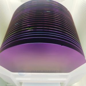
FZ Silicon Wafer

The size of float zone (FZ) silicon (Si) wafers for sale is mainly 8 inches and 6 inches. Compared with silicon wafers made by Czochralski (CZ) method, the biggest feature of float zone wafer is that the resistivity is relatively high, the purity is higher, and it can withstand high voltage. However, it is difficult to produce large-size FZ silicon wafers and the mechanical properties are poor. Therefore, there is few floating-zone grown silicon wafer used in integrated circuits. The FZ Wafer is prepared by float zone process. Because of no crucible during the float zone silicon crystal growth, the pollution from crucible is avoided, and the suspension zone melting can be used for multiple purifications, so the purity of FZ silicon ingot is high, and the conductivity of FZ-Silicon substrate can reach 1000 Ω-cm or more.
- Description
- Inquiry
Description
FZ Si wafers produced by FZ wafer suppliers are used for manufacturing power electronic devices, photodiodes, ray detectors, infrared detectors, etc. The oxygen content of FZ silicon wafer is 2~3 orders of magnitude lower than that of CZ silicon. Since there is no deposition formed by oxygen, the mechanical strength of float zone silicon wafer is not so good as well as silicon wafer CZ grown. In addition, warpage and defects are easy to generate during the fabrication process. Adding nitrogen is one solution to improve the wafer strength during the float zone silicon crystal growth. More FZ monocrystalline silicon specifications are as follows:
1. 8 inch High Resistivity Float Zone Silicon Wafer with SSP or DSP
| 8 inch FZ Silicon Wafer with SSP or DSP & Hight Resistivity | |||
| Item | Parameters | ||
| Material | Monocrystalline Silicon | ||
| Grade | Prime Grade | ||
| Growth Method | FZ | ||
| Diameter | 8″(200.0±0.2mm) | ||
| Conductivity type | N Type | N Type | P Type |
| Dopant | Phosphorus | Phosphorus | Boron |
| Orientation | [100]±0.5° | ||
| Thickness | 625+/- 5µm | 725±25μm | 725±25μm |
| Resistivity | >8,000-14,000Ωcm | >10,000Ωcm | 5,000-10,000Ωcm |
| RRV | <40% (ASTM F81 Plan C) | ||
| SEMI STD Notch | SEMI STD Notch | ||
| Surface Finish | 1SP, SSP One-Side-Epi-Ready-Polished Back Side Etched |
||
| Edge Rounded | Per SEMI Standard Metrology edge exclusion(lpd’s, mechanical parameters) 3 mm |
||
| Particle | LPDs >= 0,30 µm (including COP’s) <=25 LPDs >= 0,20 µm (including COP’s) <=30 LPDs >= 0,16 µm (including COP’s) <=60 |
||
| Roughness | <0.5nm | ||
| TTV | <1.5um | <10um | <6um |
| Bow/Warp | <35um | Bow<40µm, Warp<60µm | <40um |
| TIR | <5µm | ||
| Oxygen Content | 11-15 PPMA | ||
| Carbon Content | <2E16/cm3 | ||
| Site Flatness | SFQD 20X20mm: 0.40um | ||
| MCC Lifetime | >1,000μs | >1,000μs | >1,000μs |
| Surface Metal Contamination (Al,Ca,Cu,Fe,Ni,Zn,Cr,Na) |
≤5E10 atoms/cm2 (Al,Ca,Cu,Fe,Ni,Zn,Cr,Na) Max 5E10/cm2 | ||
| Dislocation Density | SEMI STD | SEMI STD | 500 max/ cm2 |
| Chips, scratches, bumps, haze, touch marks, orange peel, pits, cracks, dirt, contamination | All None | ||
| Laser Mark | SEMI STD | Option Laser Serialized: Shallow laser |
Along The Flat On The Front Side |
2. 6 inch FZ Silicon Wafer
| 6 inch FZ Silicon Wafer | |||
| Item | Parameters | ||
| Material | Monocrystalline Silicon | ||
| Grade | Prime Grade | ||
| Growth Method | FZ | ||
| Diameter | 6″(150 ± 0.5mm) | ||
| Conductivity type | Intrinsic | N Type | P Type |
| Dopant | low doped | Phosphorus | Boron |
| Orientation | <100>±0.5° | [100]±0.5° | (111)±0.5° |
| Thickness | 625±15μm | 675±10μm 1,000±25µm |
875±25μm 1,000±25µm |
| Resistivity | >20,000Ωcm | 6,000-10,000 | 5,000-10,000Ωcm |
| RRV | <40% (ASTM F81 Plan C) | ||
| Primary Flat | One SEMI Flat (57.5mm) | SEMI STD | SEMI Notch @ 110 ± 1° |
| Secondary Flat | N/A | SEMI STD | N/A |
| Surface Finish | Front side finish Mirror Polish Back side finish Mirror Polish |
Front side finish Mirror Polish Back side finish Mirror Polish |
One Side Polished Back Side Acid Etched |
| Edge Rounded | Per SEMI Standard | ||
| Particle | <20counts @0.3μm | ||
| Roughness | <0.5nm | ||
| TTV | <10um | <10um | <12um |
| Bow/Warp | <30um | <40um | <60um |
| TIR | <5µm | ||
| Oxygen Content | <2E16/cm3 | ||
| Carbon Content | <2E16/cm3 | ||
| OISF | <50/cm² | ||
| STIR (15x15mm) | <1.5µm | ||
| MCC Lifetime | >1,000μs | ||
| Surface Metal Contamination Na, Al, K, Fe, Ni, Cu, Zn |
≤5E10 atoms/cm2 | ||
| Dislocation Density | 500 max/ cm2 | ||
| Chips, scratches, bumps, haze, touch marks, orange peel, pits, cracks, dirt, contamination | Tarnish, orange peel, contamination, haze, micro scratch, chips, edge chips, crack, crow feet, pin hole, pits, dent, waviness, smudge&scar on the back side: all none | ||
| Laser Mark | Along The Flat On The Front Side,Option Laser Serialized: Shallow laser |
||
3. 6 inch FZ+NTD Silicon Wafer with Minority Carrier Lifetime 300μs
| 6 inch FZ+NTD Silicon Wafer with Minority Carrier Lifetime 300μs | |
| Description | Requirements |
| General characteristics | |
| Method of growing | Grown by irradiating low doped Float Zone silicon with neutrons FZ+NTD |
| Orientation | <111> +/- 1 deg |
| Typ of conductivity | N |
| Impurity substance | P |
| Area of the control | 3 mm from border of a wafer are not supervised |
| The electrical characteristics | |
| Resistivity constant | 100 Ohm.cm ±8% |
| Radial dispersion of resistivity constant |
No more than 4 % |
| Minority Carrier Lifetime min |
300 mcs |
| The chemical characteristics | |
| Content of oxygen | 0.2 ppma |
| Content of carbon | 0.2 ppma |
| Perfection of structural | |
| Dislocation content | free |
| Defect density of package | No more than 1*102 1/cm2 |
| Microdefect density | No more than 1*104 1/cm2 |
| Swirls | free |
| Characteristic of wafers preparation | |
| Back side | Lapped and etching |
| Geometrics | |
| Diameter | 152,4+1 mm |
| Stretch of primary cut | 30-35 mm |
| Breadth of facet | 0,1-0,25 mm production on a «former» |
| Thickness | 625 um |
| Polythickness (TTV) | no more than 5 um |
| Warpage | No more than 35 um |
| Variation in plane | No more than 5 um |
| Surface of work condition | Polished |
| Scratchs | Deficiency |
| Microscratch (risk) | Total length no more than 0,5 diameters of a wafer |
| Contamination | Deficiency |
| Dulling | HAZE≤5 ppm |
| Scabbings | Deficiency |
| Orange peel | Deficiency |
| Saw blade defect | Deficiency |
| Surface of not work condition | Ground, Etched |
| Scabbings border | Deficiency |
| Crack such “crow’s claw” | Deficiency |
| Contamination | Deficiency |
| Saw blade defect | Deficiency |
| Scratchs | Total length no more than 0,5 diameters of a wafer |
| Speck from non-uniform etching | Deficiency |
4. 6 inch FZ+NTD Silicon Wafer with Orientation (111) & Thickness 625μm
| 6 inch FZ+NTD Silicon Wafer with Orientation (111) & Thickness 625μm | |||
| Description | Unit | Value | Standard of Control Method |
| Method | FZ+NTD | ||
| Type | N | ||
| Dopant | P ( Phosphorus) | ||
| Orientation | — | <111> +/- 1 deg | ASTM F 26 |
| Diameter | mm | 152.4±1 | Caliber |
| Thickness, min | um | 625 | — |
| Resistivity | Ohm*cm | 100 | 4-point probe ASTM F 84 |
| Radial Resistivity Variation, max | % | 8 | ASTM F 81 Plan C |
| Minority Carrier Lifetime, min | mcs | 300 | ASTM F1535-94 |
| Carbon Content, max | ppma | 0.2 | ASTM F 1391-93 |
| Oxygen Content/ | ppma | 0.2 | ASTM F 1188-93a |
| Front side | Polished | ||
| Back side | Ground, Etched | ||
| Swirls | — | none | F47 |
| Dislocations | — | none | F47 |
5. 6 inch FZ+NTD Silicon Wafer with Thickness 300μm
| 6 inch FZ+NTD Silicon Wafer with Thickness 300μm | |
| Description | Requirements |
| Diameter | 150mm±0.5mm |
| Thickness | 300um |
| Growth method | FZ+NTD |
| Orientation | (100) |
| Type: N | N |
| Dopant | P |
| Resistivity | 85 Ohm*cm ±4% |
| Surface Finish | Single side polished |
| Flats | 1, SEMI-Std, length 30-35mm |
| TTV | ≤5um |
| Warp | ≤35um |
| Bow | ≤5um |
| Oxygen content | ≤1.0*10^18cm-3 |
| Carbon content | ≤5.0*10^16cm-3 |
| Dislocations | None |
| Slip | None |
| Haze | None |
| Scratches | None |
| Edge Chips | None |
| Dimples | None |
| Orange Peel | None |
| Cracks/Fractures | None |
6. 6 inch FZ+NTD Silicon Ground Ingot
| 6 inch FZ+NTD Silicon Ground Ingot | |||
| Parameter | Unit | Value | Standard of Control Method |
| Method | FZ+NTD | ||
| Type | N | ||
| Dopant | P ( Phosphorus) | ||
| Orientation | — | <111> +/- 1 deg | ASTM F 26 |
| Diameter | mm | 150.0+0.5 | Caliber |
| Resistivity | Ohm*cm | 170 | 4-point probe ASTM F 84 |
| Radial Resistivity Variation, max | % | 8 | ASTM F 81 Plan C |
| Minority Carrier Lifetime, min | mcs | 300 | ASTM F1535-94 |
| Carbon Content, max | ppma | 0.2 | ASTM F 1391-93 |
| Oxygen Content | ppma | 22 | ASTM F 1188-93a |
| Swirls | — | none | F47 |
| Dislocations | — | none | F47 |
7. 4 inch FZ Silicon Wafer
| 4 inch FZ Silicon Wafer | |||
| Item | Parameters | ||
| Material | Monocrystalline Silicon | ||
| Grade | Prime Grade | ||
| Growth Method | FZ | ||
| Diameter | 4″(100±0.4mm) | ||
| Conductivity type | Intrinsic | N Type | P Type |
| Dopant | low doped | Phosphorus | Boron |
| Orientation | <111>±0.5° | [110]±0.5° | (100)±1° |
| Thickness | 500±25μm | ||
| Resistivity | >10,000Ωcm | >5,000Ωcm | 5,000-10,000Ωcm |
| RRV | <40% (ASTM F81 Plan C) | ||
| Primary Flat | SEMI STD Flats | ||
| Secondary Flat | SEMI STD Flats | ||
| Surface Finish | One-Side-Epi-Ready-Polished, Back Side Etched |
||
| Edge Rounded | Per SEMI Standard | ||
| Particle | <20counts @0.3μm | ||
| Roughness | <0.5nm | ||
| TTV | <10um | ||
| Bow/Warp | <40um | ||
| TIR | <5µm | ||
| Oxygen Content | <2E16/cm3 | ||
| Carbon Content | <2E16/cm3 | ||
| OISF | <50/cm² | ||
| STIR (15x15mm) | <1.5µm | ||
| MCC Lifetime | >1,000μs | ||
| Surface Metal Contamination Fe,Zn, Cu,Ni, K,Cr | ≤5E10 atoms/cm2 | ||
| Dislocation Density | 500 max/ cm2 | ||
| Chips, scratches, bumps, haze, touch marks, orange peel, pits, cracks, dirt, contamination | All None | ||
| Laser Mark | Along The Flat
On The Front Side, Option Laser Serialized: Shallow laser |
||