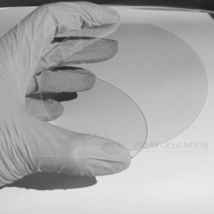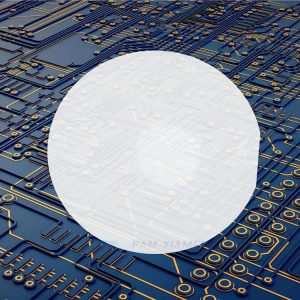
Semi-Insulating Freestanding GaN Substrate

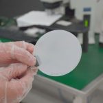
Semi-insulating Freestanding GaN (Gallium Nitride) Substrate is mainly for RF device based on HEMT structure. Ganwafer, a semi-insulating freestanding GaN substrate manufacturer, has formed the manufacturing technology for freestanding GaN semi-insulating substrate wafer. The substrate wafer is for UHB-LED and LD. Our GaN substrate grown by hydride vapor phase epitaxy (HVPE) has low defect density and less or free macro defect density. More specification of GaN semi-insulating substrate, please see below:
- Description
- Inquiry
Description
1. Specification of Semi-insulating Freestanding GaN Substrate
1.1 4″ Semi-Insulating GaN Wafer Substrate
| Item | GANW-FS-GaN100-SI |
| Conduction Type | Semi-Insulating |
| Size | 4″(100)+/-1mm |
| Thickness | 480+/-50um |
| Orientation | C-axis(0001)+/-0.5° |
| Primary Flat Location | (10-10)+/-0.5° |
| Primary Flat Length | 32+/-1mm |
| Secondary Flat Location | (1-210)+/-3° |
| Secondary Flat Length | 16+/-1mm |
| Resistivity(300K) | >10^6Ω·cm |
| Dislocation Density | <5×106cm-2 |
| FWHM | <=100arc.sec |
| TTV | <=30um |
| BOW | <=+/-30um |
| Surface Finish | Front Surface: Ra<=0.3nm.Epi-ready polished |
| — | Back Surface: 1. Fine ground |
| — | 2. Polished |
| Usable Area | ≥ 90 % |
1.2 2″ Semi-Insulated GaN Free-standing Substrate
| Item | GANW-FS-GaN50-SI |
| Conduction Type | Semi-Insulating |
| Size | 2″(50.8)+/-1mm |
| Thickness | 400+/-50um |
| Orientation | C-axis(0001) off angle toward A-axis 0.35°+/-0.15° |
| Primary Flat Location | (10-10)+/-0.5° |
| Primary Flat Length | 16+/-1mm |
| Secondary Flat Location | (1-210)+/-3° |
| Secondary Flat Length | 8+/-1mm |
| Resistivity(300K) | >10^6Ω·cm |
| Dislocation Density | <5×106cm-2 |
| FWHM | <=100arc.sec |
| TTV | <=15um |
| BOW | <=+/-20um |
| Surface Finish | Front Surface: Ra<=0.3nm. Epi-ready polished |
| — | Back Surface: 1. Fine ground |
| — | 2. Polished. |
| Usable Area | ≥ 90 % |
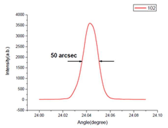
2. XRD Rocking Curves-GaN Material-TEST REPORT
A test report can show the wafer quality and the concordance between description and data of wafers. After the manufacturing process, we will test the wafer characterization:
* Test wafer surface roughness by atomic force microscope;
* Test conductivity type by Roman spectra instrument;
* Test wafer resistivity by non-contact resistivity testing equipment;
* Test micropipe density of wafer by polarizing microscope.
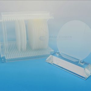
We will clean and pack the wafers in 100 class clean environment after testing. If the qualities of the wafers do not meet the custom spec, we will take it off after the testing.
The half-height full width (FWHM) is the spectral curve width measured between those points on the Y-axis. Following diagram shows the XRD Rocking Curves of GaN Material tested:
Remark:
The Chinese government has announced new limits on the exportation of Gallium materials (such as GaAs, GaN, Ga2O3, GaP, InGaAs, and GaSb) and Germanium materials used to make semiconductor chips. From August 1, 2023 on, exporting these materials is only allowed if we obtains a license from the Chinese Ministry of Commerce. Hope for your understanding!