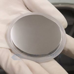
Compound semiconductor materials, like GaAs compound, GaSb compound, InAs compound, InSb compound, InP compound, are provided with high electron mobility.
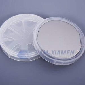
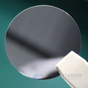
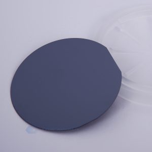
Compound semiconductor is compounds formed by two or more elements in a definite atomic ratio, and have certain semiconductor properties such as a forbidden band width and an energy band structure. The industry chain can be divided into wafer preparation, chip design, chip manufacturing, and chip packaging and testing. Wafer preparation is further subdivided into two parts: compound semiconductor substrate preparation and compound semiconductor epitaxial wafer preparation.
Metal organic vapor phase epitaxy (MOVPE) is the most popular technique for compound semiconductor foundry to form compound semiconductor thin films for devices. Moreover, technologies such as MBE, HVPE, LPE, MOMBE and ALD can be used for the growth of compound semiconductor materials.
At present, with the gradual maturity of ALD technology, the quality and reliability of devices based on HMET structures and MOSFET structures on compound semiconductor n type, p type or semi-insulating type have been greatly improved, further improving the occupation rate of compound semiconductor materials market in the field of high-frequency and high-voltage applications.
Regarding compound semiconductor applications, the semi-conductors are mainly used in following fields:
Optoelectronic devices: the main optoelectronic applications of compound semiconductor substrate include solar cells, semiconductor lighting, lasers and detectors, etc;
Microwave radio frequency: the main application of compound semiconductor wafers is radio frequency power amplifiers;
Power devices: compound wafers are mainly used in high-voltage switching devices. Compared with traditional Si process devices, compound semiconductor devices have higher power density, lower energy loss and better high-temperature stability.
Compound Semiconductor
Copyright◎2021 Ganwafer All Right Reserved