Sapphire-based Blue LED GaN Epi Structure
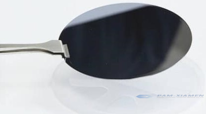
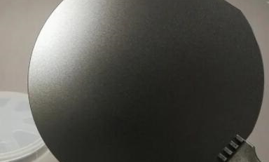
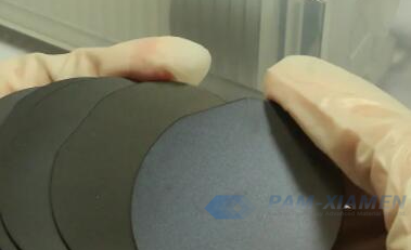
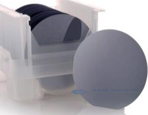
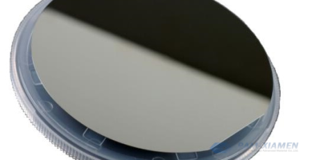
Currently, in the preparation of blue LEDs, gallium nitride (GaN) materials are usually grown by means of heteroepitaxy. In commercial GaN based LED, most of them use sapphire as the substrate material for epitaxial growth. There is a band gap in the gallium nitride semiconductor, and wavelengths can easily be shifted from the green to the blue by adding indium (shift to longer wavelengths) or aluminum (shift to shorter wavelengths). The parameters of blue LED GaN epitaxy on patterned sapphire substrate from Ganwafer are shown as follows:
1. 4 inch LED GaN Epi-on-Sapphire Wafer Specification
GANW220421-GOSLED
| Epitaxy | |
| Material | GaN |
| Area used | > 90% |
| Dislocation density | xx cm2 |
| Thickness of p-GaN | xx um |
| Carriers concentration of p-GaN | xx |
| Carriers mobility of p-GaN | xx |
| WLD | 450-460 nm |
| Tolerance | xx nm |
| Light output power (at current 20 mA) | xx mW |
| Substrate | |
| Material | PSS sapphire |
| Diameter | 4” (100 mm) |
| Thickness | 650±25um |
| Orientation | C-plane(0001)0°±0.5° |
| Primary flat length | 30±1.5 mm |
| Primary flat orientation | A-plane(11-20) 0°±0.25° |
| Bow | <20 um |
| WARP | <10 um |
| TTV | <20 um |
| Laser marking | backside |
| Polishing front side | epi-ready, Ra<0.2 nm |
| Polishing back side | fine ground |
2. Performance of GaN-on-Sapphire LED
The performance of gallium nitride LED mainly has two advantages, namely, the internal quantum efficiency (IQE) of the active region and the high light extraction efficiency. The result of low internal quantum efficiency is affected by the high thread dislocation (TD) density of LED GaN films grown on hetero-substrates. TDs are metal materials that form electron diffusion paths into the active layer. Due to the weaker matrix localization, the light emission efficiency is more sensitive to the non-radioactive recombination center of the TD when the emission wavelength is shortened. In order to improve the light extraction efficiency of GaN based LED, several solutions are suggested below.
3. How to Improve Light Extraction Efficiency of GaN Blue LED?
At present, the main ways to improve the external quantum efficiency of LED devices on GaN-on-Sapphire are distributed Brag reflector (DBR), substrate laser lift-off (LLO), changing LED geometry and flip chip (Flip Chip), surface roughening, photonic crystal, surface plasmon and the use of chip microstructure, etc.
Take the photonic crystal for example. The use of photonic crystals to improve the extraction efficiency of LED has the advantages of simple process and high light extraction efficiency, so it has become one of the research hotspots to improve the external quantum efficiency of LEDs, such as Micro LED. There are two main mechanisms to improve the light extraction efficiency of LEDs:
(1) Diffraction mechanism, which is mainly used in photonic crystal structures with relatively large lattice constants;
(2) Band gap mechanism, it is the band gap condition at which the lattice constant reaches the GaN LED wavelength
In terms of photonic crystal, there are three main methods currently adopted for improving light extraction efficiency of GaN LED structure:
One is to fabricate a two-dimensional structure on the surface of p-type GaN material or Indium-Tin-Oxide (ITO) layer to improve the light extraction efficiency of the device;
The other is to use the bottom surface of sapphire substrate, making a lens array-like structure to improve the light extraction efficiency of the LED GaN bottom surface;
The third is to make a two-dimensional structure on a PSS sapphire substrate, and then grow GaN LED wafer to make related devices.
For more information, please contact us email at sales@ganwafer.com and tech@ganwafer.com.


