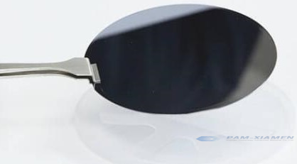
InSb Wafer Market in Photonic Cooled Infrared Detector
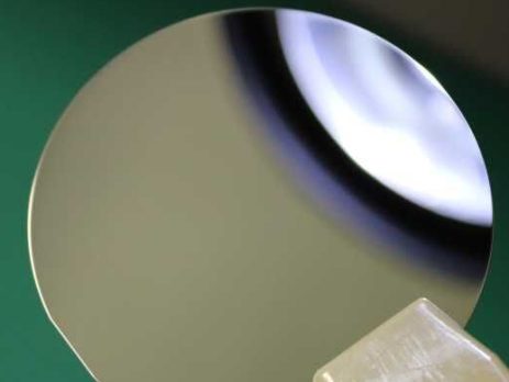
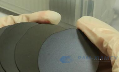
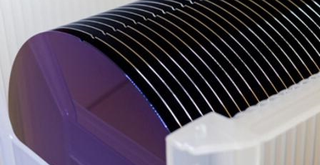
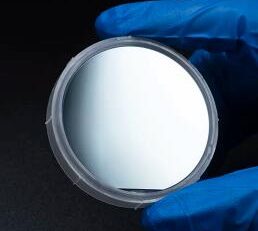
Indium antimonide (InSb) has the characteristics of the lowest melting point, narrow band gap, high carrier mobility, and good structural integrity. It is a special compound among III-V semiconductor compounds. These properties facilitate the broad applications of indium antimonide as substrate for optoelectronic devices and infrared detectors in the 3-5 um range. InSb-based photodetector arrays have high uniformity, contain a large number of working cells, and are less expensive than similar devices based on HgCdTe (MCT). All the advantages make InSb a key material for fabricating large mid-infrared arrays. Ganwafer can provide InSb wafer for making photoelectron detectors.
InSb detectors started in the 1950s, multi-element and linear detectors were developed in the 1960s, and focal plane detectors were developed in the 1980s, and they were basically mature in the 1990s. At present, it is developing in the direction of smaller photosensitive element size and larger array scale. InSb has the characteristics of high quantum efficiency and good stability, and currently occupies a dominant position in military medium-wave infrared detector systems. Compared with HgCdTe, InSb focal plane array material has low defect density and low dislocation density; InSb material does not have the problem of composition uniformity, the crystal size is larger, the uniformity is higher, and the resulting detector spectrum and Non-uniformity of response; InSb wafer is a standard wafer, which can realize automatic chip production, low device cost, high long-term stability, and strong competitiveness in system applications.
1. InSb Wafer Market Share in Photonic Cooled IR Detector
According to Maxtech International analysis, the global photonic infrared detector market is expected to reach US$7.2 billion by 2023, with InSb detectors taking the first market share. Please refer to Figure 1 & 2 for specific data:
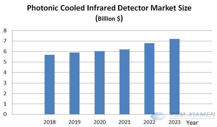
Figure 1: Global Market Size of Photonic Cooled Infrared Detectors (Data from Maxtech International)
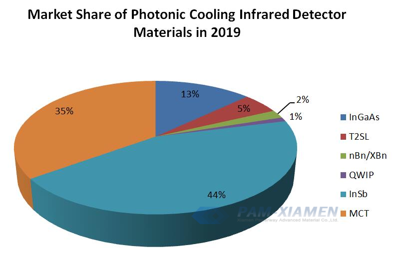
Figure 2: Market Share of Photonic Cooling Infrared Detector Materials in 2019 (Data from Maxtech International)
2. Application Fields of InSb Thermal Vision System
The key structural element of the high-sensitivity long-distance thermal vision system is the photodetector array based on indium antimonide material. These devices work by converting the thermal radiation of an object into a visible image, i.e. the release of heat from a mask or concealment to make it visible. In recent years, thermal vision systems have penetrated deeper and deeper into various fields, and their application fields have been greatly expanded.
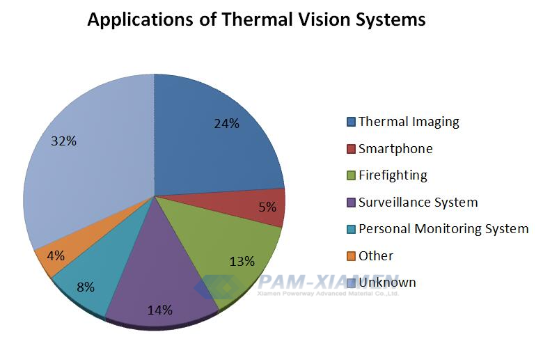
Figure 3: Applications of Thermal Vision Systems (Data from Yole)
Compared with other III-V compounds, the design of optoelectronic devices based on InSb materials has driven the main trend in the research and development of indium antimonide. The fabrication of photodetector arrays for high-resolution identification of all-optical images and the need to improve device yields place new demands on the diameter, structural perfection, and uniformity of electrophysical properties of the single crystals used in the process.
For more information, please contact us email at sales@ganwafer.com and tech@ganwafer.com.

